Explore our premium medical-grade phototherapy devices, custom engineered with clinical wavelengths (415nm to 1064nm) for targeted dermatological and tissue repair protocols.
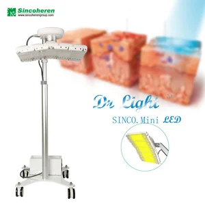
How precise optical wavelengths are disrupting the global body care, beauty wellness, and rehabilitation markets.
The global demand for LED body care devices has evolved from simple aesthetic enhancements to scientifically backed medical-grade treatments. Known in clinical research as Photobiomodulation (PBM) or Low-Level Light Therapy (LLLT), this technology employs specific bands of the electromagnetic spectrum to trigger cellular metabolic processes. When photons are absorbed by cytochrome c oxidase within the mitochondria of dermal and muscle cells, ATP production increases, microcirculation accelerates, and collagen synthesis is up-regulated.
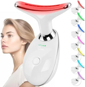
B2B distributors and beauty brands must understand the physiological impact of different wavelengths to optimize their portfolios. The standard protocol for skin rejuvenation and systemic inflammation mitigation centers on 630nm to 660nm (Red Light) and 830nm to 850nm (Near-Infrared Light). Red light addresses epidermal cells to alleviate fine lines and enhance skin elasticity, while near-infrared light penetrates deeper into subcutaneous tissues, joints, and muscle groups to assist with deep tissue repair and inflammation reduction.
According to clinical data, optical power density—referred to as irradiance—is the primary indicator of device efficacy. Low irradiance (below 20mW/cm²) yields suboptimal results, requiring excessive exposure times. Conversely, overly high irradiance without professional thermal management can cause thermal damage to the skin barrier. For these reasons, global procurers look to expert manufacturers like Guangzhou TK Beauty Co., Ltd., who construct optical devices with highly targeted irradiance and tight spectral tolerances (±5nm).
Strict verification of optical energy output (mW/cm²) at standardized distances, ensuring deep tissue penetration and therapeutic energy delivery.
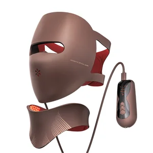
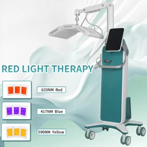
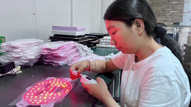
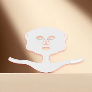
Custom combinations of 415nm (blue), 590nm (yellow), 660nm (red), and 850nm/1064nm (NIR) light, optimized for varied skin depth treatments.
Integrated cooling systems and copper PCB backplanes prevent heat degradation of LED chips, maintaining long-term stability and safety.
Guangzhou TK Beauty Co., Ltd. is a professional China LED Beauty Device Manufacturer specializing in advanced light therapy technology, skincare innovation, and beauty device solutions for global beauty brands, distributors, retailers, e-commerce businesses, and private label companies. With a commitment to technological innovation and product excellence, we provide high-performance beauty devices designed to meet the growing demand for effective and convenient at-home skincare solutions.
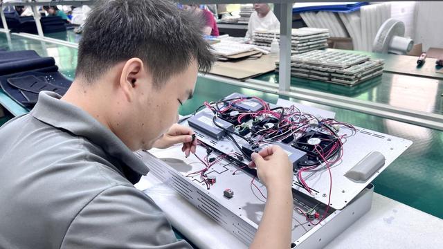
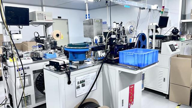
Operating out of the primary electronic manufacturing hub in Guangdong, TK Beauty utilizes a highly optimized ecosystem for components sourcing, PCB assembly, and advanced optical calibration. The company offers comprehensive OEM and ODM manufacturing services, helping B2B partners develop custom form factors, tailored wavelengths, and bespoke remote-control interfaces from concept to final distribution.
TK Beauty ensures that quality, safety, and reliability are at the core of all manufacturing processes. Our production facilities operate under strict quality management systems and utilize advanced manufacturing equipment to ensure consistent product performance and compliance with international standards. Continuous investment in research and development allows us to stay at the forefront of emerging beauty technology trends and deliver innovative solutions to customers worldwide.
Understanding medical-grade silicone selection and wavelength precision in professional LED body devices.
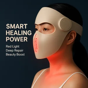
In modern light therapy, the hardware materials are just as important as the electronic components. Flex-style phototherapy devices, such as wearable wraps, masks, and pads, are in direct contact with skin and must utilize biocompatible materials. TK Beauty uses only medical-grade liquid silicone that has undergone biocompatibility testing for skin irritation and cytotoxicity. This ensures comfortable, safe application on sensitive skin over extended treatment periods.
Simultaneously, the optical engineering of these devices relies on high-grade semiconductor dies. Lower-tier manufacturers may use generic LEDs that shift in color output under thermal stress. TK Beauty devices are built with gold-wire bonded LED chips mounted to thick aluminum or copper printed circuit boards. This structure maximizes heat dissipation, preventing wavelength drift and keeping the light output stable at critical bands like 660nm and 850nm.


Key standards for launching and distributing LED wellness devices across North American, European, and Asia-Pacific markets.
Distributing high-performance personal care and wellness devices globally requires strict adherence to international safety and electromagnetic standards. Because LED body care devices are powered and emit electromagnetic energy, they must pass rigorous testing before entering major retail networks. A professional supplier must provide complete documentation to ensure smooth clearance through customs and protect retail partners from liability.
The regulatory framework for these devices includes:
Guangzhou TK Beauty Co., Ltd. addresses these regulatory requirements with a dedicated compliance team. From initial PCB layout design to final casing assembly, every step is aligned with these international certifications. This proactive approach helps brands reduce development risks and launch new products on schedule.
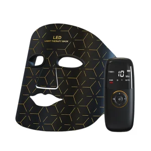
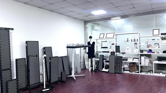
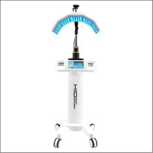
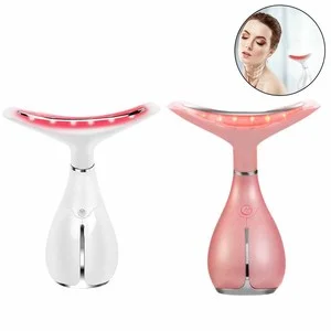
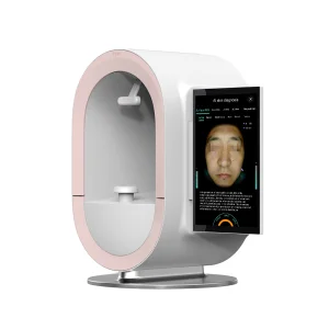
Review our professional-grade solutions, including wearable wraps, localized phototherapy tools, and high-performance salon equipment.
Detailed answers to key engineering, compliance, and B2B ordering questions.
A: We test every production batch using an integrating sphere and high-resolution spectroradiometer. Irradiance mapping is performed at distances of 0cm, 5cm, and 10cm. We supply verified irradiance reports (typically ranging from 30mW/cm² to 120mW/cm² depending on the model) to guarantee therapeutic performance.
A: Yes. Our engineering team can configure custom spectrums tailored to your target application. Typical custom configurations include 415nm (acne control), 590nm (pigmentation reduction), 660nm (collagen stimulation), 850nm (muscle recovery), and 1064nm (deep tissue therapy).
A: We use high-conductivity aluminum or copper printed circuit boards (PCBs) combined with silicone materials that offer low thermal resistance. In our high-power systems, we integrate silent fans to keep junction temperatures low, ensuring the emission spectrum remains within a tight tolerance of ±5nm.
A: Our products are manufactured to meet CE, RoHS, and FCC regulations. Additionally, we use biocompatible medical-grade silicone that has completed ISO 10993 testing. We work closely with our partners to provide the necessary documentation for FDA registrations and CE-MDR compliance.
A: For standard OEM projects with logo printing and packaging modifications, the typical lead time is 25-30 days. For custom ODM projects requiring new industrial design, mold injection, and PCB engineering, the process takes approximately 60-90 days, including prototype validation.