Advanced optoelectronic parameters optimized for dermatological luminosity, cell renewal, and transdermal penetration technologies.
Strategic positioning of Guangzhou TK Beauty Co., Ltd. as the pioneer in high-density LED luminosity engineering.
How the Pearl River Delta industrial ecosystem optimizes capitalization, procurement agility, and technological time-to-market.
Located within the epicenter of global electronic manufacturing, our supply chain incorporates hyper-localized access to raw SMD LED chip semiconductor fabrication, precision injection molding, and surface-mount technology (SMT) automated pipelines, reducing component lead times to near-zero margins.
Unlike lower-tier providers, our production matrices are strictly mapped to international compliance protocols. We provide fully documented FDA clearance pathways, CE-Medical directives, RoHS structural validation, and comprehensive IEC 62471 photobiological safety certification for optical radiation.
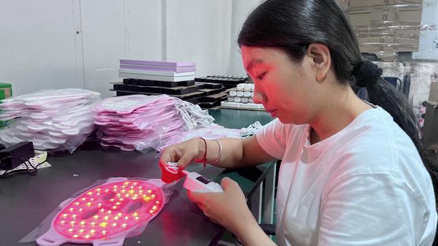
Every unit undergoes strict radiometric and spectroradiometric evaluation using integrating spheres and high-precision goniophotometers. We continuously measure and audit optical power density (irradiance output in mW/cm²) to ensure uniform energy spatial distribution across the target epidermis.
A common industry misconception propagated by amateur distributors is that a higher volume of individual LED chips linearly equates to greater clinical efficacy. Our engineering team has mathematically demonstrated that total energy delivery relies entirely on Targeted Spectral Irradiance ($mW/cm^2$) and thermal stability, rather than crude chip count. A device with 100 highly calibrated, narrow-band LEDs backed by premium copper substrate PCBs will yield 300% deeper dermal penetration and skin luminosity enhancement compared to a 500-chip budget counterpart experiencing thermal degradation and wide-spectrum wavelength bleeding.
Anticipating macro shifts in consumer behavior and advanced biomedical device engineering paradigms.
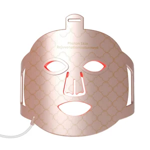
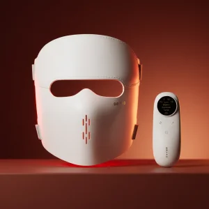
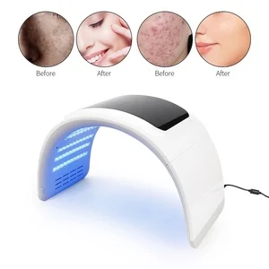
The market is migrating rapidly away from basic single-wavelength modes. Next-generation systems employ synchronized sequential pulses alternating between 630nm (superficial epidermal smoothing), 660nm (deep dermal neocollagenesis initiation), and 850nm (near-infrared hypodermal cellular resonance), providing multifaceted luminosity enhancement in single treatment protocols.
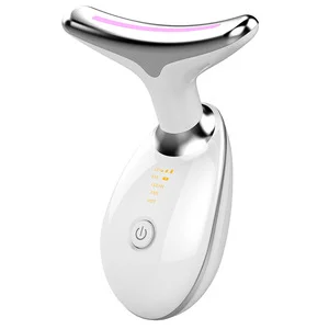
Engineering modern form factors requires the flawless amalgamation of variable radio frequency thermal tissue tightening, low-frequency electrical muscle stimulation for facial contour muscle toning, and high-density LED arrays. This concurrent synergy drastically elevates skin-elasticity indexes and speeds up cellular turnover cycles.
Advanced consumer ecosystems demand intelligent customization. Our ongoing R&D investments focus on integrating high-fidelity dermal moisture/pigment sensor nodes within silicone matrices. These sensors relay real-time localized physiological data to dedicated smartphone software, dynamically adjusting irradiance energy dose profiles on a user-by-user basis.
Tailoring optoelectronic physical designs to match specialized global consumer operational environments.
Demands lightweight, highly ergonomic configurations, wireless inductive charging architectures, and food-grade ultra-flexible silicone materials that guarantee multi-point flush contact across varied cranial dimensions without causing nasal or ophthalmic pressure points.
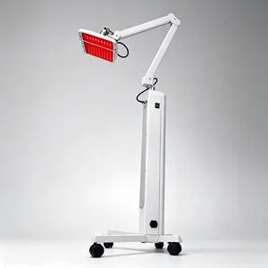
Requires heavy-duty, multi-joint articulation arm setups, high-output static panels (such as our 275W/6000W architectures), rapid cooling heatsink assemblies for consecutive back-to-back treatment runs, and sterile, chemical-resistant exterior coatings to withstand medical sanitization fluids.
Requires highly compressible flat-pack shapes, global voltage-compatible USB-C power delivery IC ports, robust haptic shock protection, and custom sleek travel pouch integrations designed to appeal to high-turnover premium consumer subscriptions.
Comprehensive breakdown of our vertically integrated OEM, ODM, and custom engineering service life cycle.
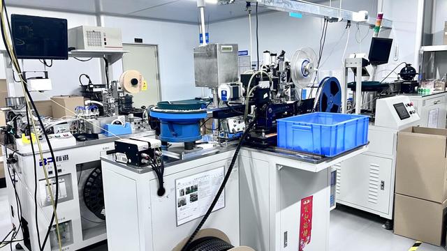
Using advanced computer-aided optical software modeling, our laboratory simulations analyze skin layer light absorption rates prior to hardware manufacturing. We pre-calculate ray-tracing paths to verify that light passing through integrated micro-lenses scatters optimally across both epidermal and subcutaneous target fields.
Our internal tooling division develops ultra-precise steel injection mold cavities, guaranteeing that complex flexible contours, latch mechanisms, and multi-pin contact modules retain seamless tactile feedback and watertight structural sealing across thousands of use cycles.
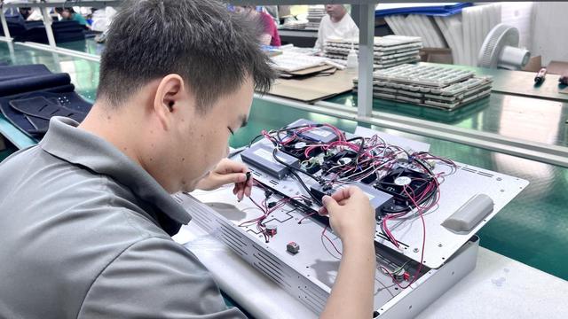
Every single manufactured electronic assembly batch undergoes a continuous 72-hour automated power-load burn-in test within temperature-controlled environmental chambers. This step ensures zero driver failure rates, consistent current-density management, and lasting durability for integrated lithium polymer battery management systems (BMS).
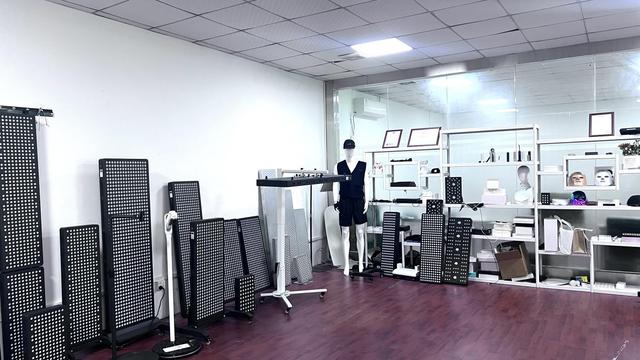
Inside our state-of-the-art manufacturing facility, where optical consistency meets surgical cleanliness standards.
Answering complex engineering, technical, and regulatory questions from enterprise buyers and supply-chain heads.
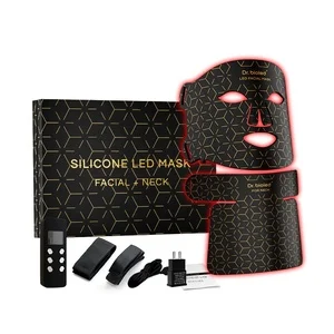
Our standard premium configurations execute clinical-grade precision at 630nm and 660nm for deep Red Light Therapy, 415nm for localized anti-microbial acne mitigation, and 850nm for deep tissue Near-Infrared (NIR) penetration. Wavelength deviation is constrained under a strict ±2nm tolerance envelope through narrow-band die sorting, completely eliminating non-therapeutic light runoff.
We design custom, highly efficient constant-current driver boards that counteract voltage drops across flexible circuits. Irradiance values are strictly audited between $30\text{ mW/cm}^2$ and $65\text{ mW/cm}^2$ depending on target positioning, measured directly at functional facial skin surface distances using an industry-standard spectroradiometer.
We supply full comprehensive technical files including CE (Medical Device Directive/MDR compliant documentation), FCC Part 15 validation, RoHS 2.0 component substance tracking sheets, and IEC 62471 photobiological eye safety certification. Additionally, we actively cooperate with enterprise clients to secure direct FDA 510(k) notification pathways.
Yes, we exclusively utilize platinum-cured, medical-grade liquid silicone rubber (LSR). It passes comprehensive ISO 10993 cytotoxicity, sensitization, and intracutaneous reactivity testing, ensuring the device remains entirely hypoallergenic, inert, and fully resistant to repeated clinical chemical cleanings.
Absolutely. Our advanced ODM ecosystem specializes in multi-modal integration. We regularly fuse high-frequency thermal Radio Frequency circuits with low-voltage localized microcurrents, arranging them seamlessly alongside high-density LED arrays while maintaining strict electromagnetic compatibility (EMC) isolation.
A standard custom project moves through industrial concept design and 3D CAD modeling in 10-14 days. Functional CNC prototyping and optical simulation require 21 days. Production tooling development takes approximately 30-35 days, followed by initial pilot-run verification within 15 days.
For high-power solutions like our 275W lamps or 6000W clinical panels, we implement thick multi-layered aluminum heat sinks and silent magnetic levitation cooling fans. For wearable silicone masks, we manage temperature via optimized current duty cycles, ensuring structural skin contact surfaces never surpass a safe $41^\circ\text{C}$ threshold.
Standard custom logo branding, specialized color paths, and retail packaging modifications carry a low entry barrier of 500 units per batch. Deep ODM structural alterations involving proprietary steel injection mold tools require a minimum contract volume of 2,000 units to offset industrial engineering tooling setups.
Scalable technological investments tailored for enterprise brand extensions, international clinical distribution, and luxury retail storefronts.