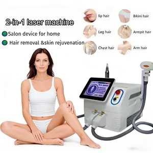
Explore our foundational array of CE-certified optoelectronic treatment systems, designed for medical-grade performance and regulatory compliance.
CE Certified Compliance
Full Lifecycle Capable
Validated Wavelengths
Logistics Network
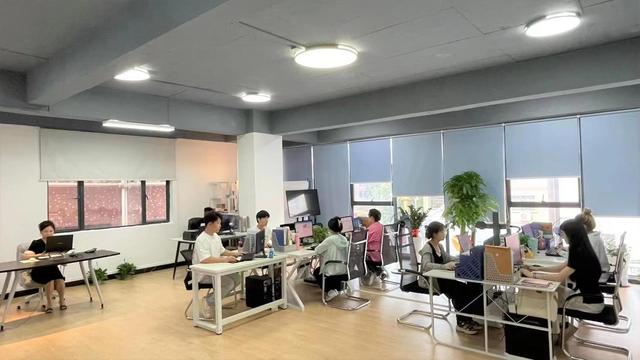
Guangzhou TK Beauty Co., Ltd. stands as a premier China LED Beauty Device Manufacturer, architecting advanced photobiomodulation and light therapy systems for demanding global markets. We support healthcare distributors, aesthetic medical networks, cross-border e-commerce enterprises, and luxury skincare entities through scientifically grounded product lines and rigorous quality control.
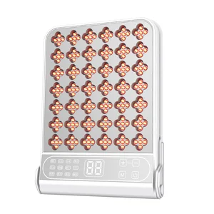
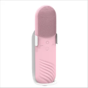
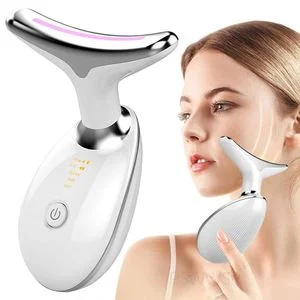
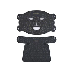
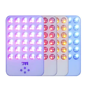
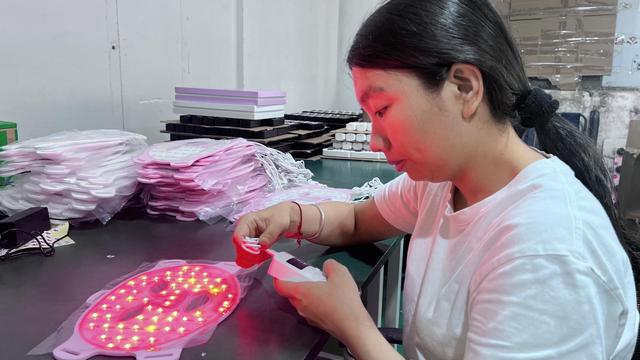
Modern photonics demand exact optical alignment, proper thermal dissipation, and accurate spectral metrics. Our product portfolio spans targeted LED wellness devices, multi-wavelength photon systems, anti-aging facial arrays, and flexible medical-grade silicone matrices. By embedding high-density LED components alongside smart control interfaces, our systems ensure consistent optical transmission and excellent user reliability.
As an engineering partner, we offer comprehensive OEM and ODM capabilities that translate client specifications into market-ready assets. From original industrial design and structural engineering to custom spectrum calibration, electronic design, and multi-tier retail packaging, we handle each phase with professional precision.
Deep-dive analysis of macro trends, technological developments, and regulatory frameworks governing the international wellness sector.
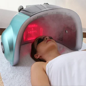
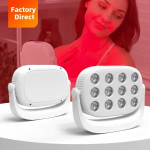
Modern clinics and consumers are transitioning from reactive treatments to proactive photobiomodulation. Safe, chemical-free therapies drive steady demand across European, North American, and Asia-Pacific markets.
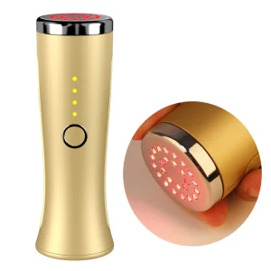
Modern product development emphasizes specific, high-purity optical outputs. Our engineering pairs 630nm/660nm red light with 810nm/830nm/850nm near-infrared wavelengths to optimize cellular absorption and mitochondrial activation.
Compliance is essential for entering professional markets. Holding legitimate CE certification confirms that our devices meet the European Union's electromagnetic compatibility (EMC) and low-voltage electrical safety mandates.
How our facility in Guangzhou combines advanced optical engineering with scaled cost efficiencies to support international partners.
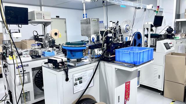
Guangzhou's industrial ecosystem provides unmatched advantages for tech manufacturing. Guangzhou TK Beauty Co., Ltd. leverages local supply chains to source premium chip components, custom tooling, and high-purity medical silicone quickly and cost-effectively. This regional advantage allows us to accelerate prototyping cycles and scale production rapidly without compromising quality.
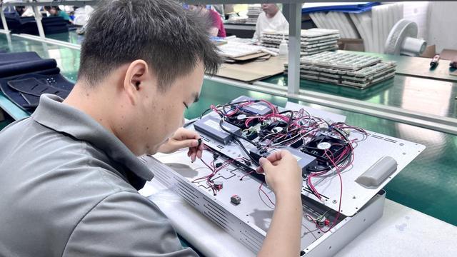
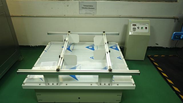
Our quality control processes include step-by-step inspections along the entire assembly line. Every production batch undergoes strict spectral calibration, thermal stress tests under load, and precise irradiance mapping. By verifying optical output power density ($mW/cm^2$) at specific distances, we ensure our devices deliver predictable, uniform performance.
Additionally, we use environmentally responsible processes throughout our facility. We comply fully with the RoHS Directive, limiting hazardous substances in our circuitry and housings, which supports clean global distribution and long-term business value.
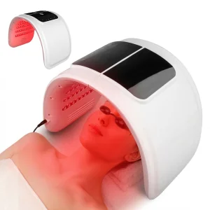
Deploying advanced light therapy technology across diverse professional spaces and high-volume commercial channels.
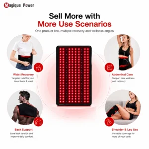
Integrating high-irradiance LED panels into recovery suites helps soothe skin, shorten downtimes, and complement specialized post-laser protocols.
We provide full-service ODM engineering, customized brand labeling, and certified packaging solutions to help brands launch market-ready wellness devices quickly.
Our structured production planning, reliable batch tracking, and vetted component supplies help distributors manage inventory costs and minimize supply chain risks.
Direct engineering answers addressing critical optical parameters, compliance standards, and production line capabilities.
Every design goes through thorough testing with calibrated spectroradiometers and integrating spheres. We screen and group individual LED components to maintain strict tolerance limits, preventing spectral drifting and ensuring predictable treatment values across our production runs.
Our CE certifications cover the Low Voltage Directive (LVD) for absolute electrical safety and the Electromagnetic Compatibility (EMC) Directive to prevent circuit interference. This complete documentation helps downstream importers pass customs inspections smoothly.
We provide full layout customization. Our engineering team can adjust optical arrays to combine different wavelengths, including 415nm blue light, 590nm yellow light, 660nm deep red light, and 850nm near-infrared light, tailored to match your specific treatment protocols.
We design our devices using high-conductivity aluminum PCBs and passive convective cooling structures. This approach limits diode junction temperatures, preventing wavelength shifts, maintaining consistent output power, and extending the operational lifespan of the LEDs.
Industrial design evaluation and 3D modeling are typically completed within 7 to 10 working days. Once tooling design is finalized, volume production runs generally require 25 to 35 days, depending on order size and custom part requirements.
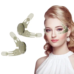
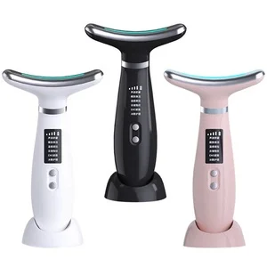
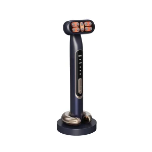
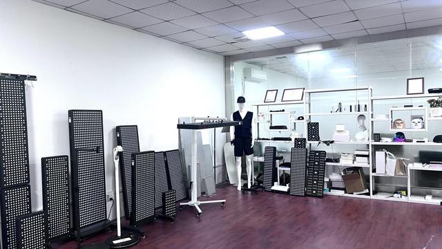
Review our specialized wearable systems and focused therapeutic options, built for high structural durability and consistent performance.